
Planar Lightwave Circuit (PLC) Technology
author: Lawson
2025-10-10
Planar Lightwave Circuit (PLC) is an optical device manufacturing technology based on planar waveguide structure. It achieves the functions of optical signal transmission, splitting, coupling, modulation, etc. by fabricating optical waveguides on planar substrates (such as silicon-based, glass based, etc.). Its core lies in utilizing the low loss and high integration characteristics of optical waveguides to integrate multiple optical functions onto a single chip, promoting the development of optical communication systems towards miniaturization and integration.
Technical Principle
A planar optical waveguide restricts the propagation of light waves in a specific medium through the principle of total internal reflection. Its typical structure is three layers:
Core layer (high refractive index materials such as silicon dioxide and lithium niobate): guides the propagation of light waves.
Cladding (low refractive index material): restricts the transmission of light waves within the core layer to prevent energy leakage.
Substrate (support layer): Provides mechanical stability.
The design of optical waveguides requires precise control of refractive index distribution and waveguide size to achieve specific optical field constraints and mode control. For example, the phase matching conditions for the formation of guided waves can be derived through X-ray analysis, ensuring that the optical path difference is an integer multiple of 2 π and compensating for the total reflection phase shift.
A planar optical waveguide restricts the propagation of light waves in a specific medium through the principle of total internal reflection. Its typical structure is three layers:
Core layer (high refractive index materials such as silicon dioxide and lithium niobate): guides the propagation of light waves.
Cladding (low refractive index material): restricts the transmission of light waves within the core layer to prevent energy leakage.
Substrate (support layer): Provides mechanical stability.
The design of optical waveguides requires precise control of refractive index distribution and waveguide size to achieve specific optical field constraints and mode control. For example, the phase matching conditions for the formation of guided waves can be derived through X-ray analysis, ensuring that the optical path difference is an integer multiple of 2 π and compensating for the total reflection phase shift.
material system
PLC technology supports multiple materials, choose according to application requirements:
Silicon dioxide (SiO ₂): low loss, high stability, commonly used in splitters and arrayed waveguide gratings (AWG).
Lithium niobate (LiNbO3): With a large transparent window, low transmission loss, and excellent electro-optical/piezoelectric properties, it is suitable for high-speed modulators and optical switches.
III-V semiconductors (such as InP, GaAs): suitable for the integration of active devices (such as lasers, detectors).
Silicon on insulator (SOI/SIMOX): compatible with CMOS processes, suitable for high-density integration.
Silicon oxynitride (SiON): Adjustable refractive index, supports multifunctional integration.
Polymer: With a wide variety of materials, simple processing, and low cost, its performance can be optimized through molecular engineering.
PLC technology supports multiple materials, choose according to application requirements:
Silicon dioxide (SiO ₂): low loss, high stability, commonly used in splitters and arrayed waveguide gratings (AWG).
Lithium niobate (LiNbO3): With a large transparent window, low transmission loss, and excellent electro-optical/piezoelectric properties, it is suitable for high-speed modulators and optical switches.
III-V semiconductors (such as InP, GaAs): suitable for the integration of active devices (such as lasers, detectors).
Silicon on insulator (SOI/SIMOX): compatible with CMOS processes, suitable for high-density integration.
Silicon oxynitride (SiON): Adjustable refractive index, supports multifunctional integration.
Polymer: With a wide variety of materials, simple processing, and low cost, its performance can be optimized through molecular engineering.
Technical advantage
1. High integration and miniaturization
The biggest breakthrough of PLC technology lies in the chip level integration of optical systems. Traditional optical systems require multiple discrete components such as lenses and prisms to be assembled through complex alignment, while PLC miniaturizes the entire optical system to the chip level, significantly reducing device size and bringing revolutionary changes to space sensitive scenarios such as 5G base stations and data centers.
2. Excellent optical performance
Through optimized waveguide design and precise manufacturing processes, PLC devices exhibit extremely low optical losses (typically below 0.1dB/cm), far superior to traditional optical components. At the same time, the device has excellent uniformity and consistency, ensuring stable and reliable signal transmission.
3. Excellent environmental stability
Using inorganic material systems such as silicon, silicon nitride, and phosphosilicate glass, PLC devices have excellent physical and chemical stability. Capable of withstanding harsh environmental conditions such as temperature changes and mechanical vibrations, with a service life of over 25 years, meeting the high reliability requirements of telecommunications grade equipment.
4. Large scale manufacturing and cost advantages
The compatibility with semiconductor processes enables PLC devices to support wafer level large-scale production. This manufacturing method not only ensures product consistency, but also rapidly reduces costs with the expansion of production scale, providing the possibility for the large-scale deployment of optical networks.
1. High integration and miniaturization
The biggest breakthrough of PLC technology lies in the chip level integration of optical systems. Traditional optical systems require multiple discrete components such as lenses and prisms to be assembled through complex alignment, while PLC miniaturizes the entire optical system to the chip level, significantly reducing device size and bringing revolutionary changes to space sensitive scenarios such as 5G base stations and data centers.
2. Excellent optical performance
Through optimized waveguide design and precise manufacturing processes, PLC devices exhibit extremely low optical losses (typically below 0.1dB/cm), far superior to traditional optical components. At the same time, the device has excellent uniformity and consistency, ensuring stable and reliable signal transmission.
3. Excellent environmental stability
Using inorganic material systems such as silicon, silicon nitride, and phosphosilicate glass, PLC devices have excellent physical and chemical stability. Capable of withstanding harsh environmental conditions such as temperature changes and mechanical vibrations, with a service life of over 25 years, meeting the high reliability requirements of telecommunications grade equipment.
4. Large scale manufacturing and cost advantages
The compatibility with semiconductor processes enables PLC devices to support wafer level large-scale production. This manufacturing method not only ensures product consistency, but also rapidly reduces costs with the expansion of production scale, providing the possibility for the large-scale deployment of optical networks.
Widely applicable scenarios
Fiber to the Home (FTTH) network
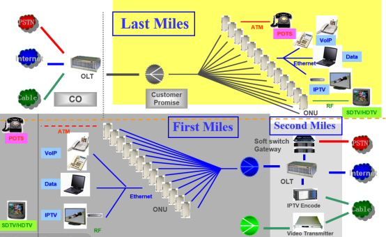
In the field of access networks, PLC optical splitters are the core components for implementing fiber to the home. It will distribute the optical signal transmitted from the central computer room to multiple end users according to a predetermined ratio, which is the key to achieving "last mile" fiber coverage. Different branching ratios ranging from 1 × 2 to 1 × 128 meet the requirements of various network architectures.
Data Center and Cloud Computing
Within the data center, PLC technology provides multiple solutions for high-speed optical interconnection. Array waveguide grating (AWG) achieves wavelength division multiplexing function, greatly improving the transmission capacity of a single optical fiber; Adjustable Optical Attenuator (VOA) ensures precise management of optical power; The optical switch matrix provides flexibility for network reconstruction.
Diversified packaging forms
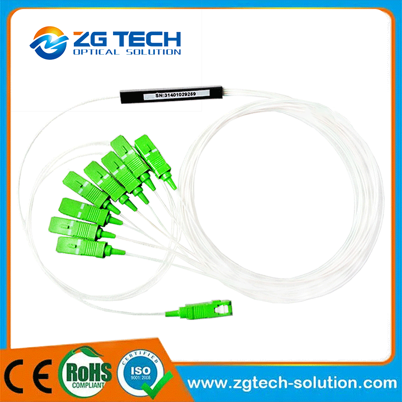
To adapt to different application scenarios, PLC devices have developed various packaging forms. Bare fiber and miniature modules are suitable for flexible deployment in indoor environments; ABS box provides good mechanical protection; The LGX box type and 1U rack type meet the high-density networking requirements, demonstrating the strong adaptability of the technology.
Fiber to the Home (FTTH) network
In the field of access networks, PLC optical splitters are the core components for implementing fiber to the home. It will distribute the optical signal transmitted from the central computer room to multiple end users according to a predetermined ratio, which is the key to achieving "last mile" fiber coverage. Different branching ratios ranging from 1 × 2 to 1 × 128 meet the requirements of various network architectures.
Data Center and Cloud Computing
Within the data center, PLC technology provides multiple solutions for high-speed optical interconnection. Array waveguide grating (AWG) achieves wavelength division multiplexing function, greatly improving the transmission capacity of a single optical fiber; Adjustable Optical Attenuator (VOA) ensures precise management of optical power; The optical switch matrix provides flexibility for network reconstruction.
Diversified packaging forms
To adapt to different application scenarios, PLC devices have developed various packaging forms. Bare fiber and miniature modules are suitable for flexible deployment in indoor environments; ABS box provides good mechanical protection; The LGX box type and 1U rack type meet the high-density networking requirements, demonstrating the strong adaptability of the technology.

Conclusion
From basic network construction to cutting-edge technological exploration, planar optical waveguide technology is becoming the core driving force for the sustainable development of the optical communication industry with its unique technological advantages. With the deepening development of the digital economy and the comprehensive promotion of new infrastructure, this mature and constantly innovative technology will play a more important role in building high-speed, intelligent, and reliable information infrastructure, injecting a continuous stream of "OPTICAL" power into the digital future.
From basic network construction to cutting-edge technological exploration, planar optical waveguide technology is becoming the core driving force for the sustainable development of the optical communication industry with its unique technological advantages. With the deepening development of the digital economy and the comprehensive promotion of new infrastructure, this mature and constantly innovative technology will play a more important role in building high-speed, intelligent, and reliable information infrastructure, injecting a continuous stream of "OPTICAL" power into the digital future.
What is a polarizing beam splitter (PBS)? ——Definition and Technical Analysis
Optical Splitters: The Silent Architects of Our Connected Worlda
Related Article


In the field of optical communication, the optical splitter plays a crucial role. However, many users may encounter issues where the optical splitter fails to ensure the efficient transmission of optical signals. This article will explore the reasons behind this problem in detail.
Why Your Optical Splitter Can't Guarantee the Transmission Efficiency of Optical Signals?