Optical Passive Devices: The Cornerstones of Modern Optical Communication Networks
Optical Passive Devices: The Cornerstones of Modern Optical Communication Networks
在数字化浪潮席卷全球的今天,光通信技术已成为信息社会的血脉,而光学无源器件则是这条血脉中不可或缺的"精密关节"。作为光通信系统的核心组成部分,这些没有光电能量转换的"沉默英雄",正以其独特的技术价值支撑着整个信息世界的高速运转。
In today's global wave of digitalization, optical communication technology has become the lifeblood of the information society, and optical passive devices are the indispensable "precision joints" of this lifeblood. As core components of optical communication systems, these "silent heroes" without photoelectric energy conversion support the high-speed operation of the entire information world with their unique technical value.
从跨洋通信干线到光纤到户(FTTH),从5G基站互联到云计算数据中心,光学无源器件在光信号的传输、分配、调度与管理中发挥着至关重要的作用。
From transoceanic communication trunks to fiber-to-the-home (FTTH), from 5G base station interconnection to cloud computing data centers, optical passive devices play a vital role in the transmission, distribution, scheduling, and management of optical signals.
精密连接的艺术:光纤活动连接器的技术进化
The Art of Precision Connection: Technological Evolution of Fiber Optic Connectors
光纤活动连接器是光网络布线的关键元件,其性能直接影响信号传输质量。当前主流产品包括FC、SC、LC等多种类型,并发展出PC、UPC、APC三种端面处理工艺。其中APC型采用8度斜面抛光技术,可将回波损耗控制在-65dB以上,显著减少反射光对激光器的影响。
Fiber optic connectors are critical components in optical network cabling, and their performance directly affects signal transmission quality. Current mainstream products include FC, SC, LC, and other types, with three end-face processing technologies: PC, UPC, and APC. The APC type, using an 8-degree angled polish technology, can control return loss to better than -65dB, significantly reducing the impact of reflected light on lasers.
陶瓷插芯作为连接器的核心部件,其加工精度达到微米级:外径公差控制在±0.5μm以内,光纤孔径精度达±0.5μm,偏心量小于1μm。这种极端精度确保了光纤对接时的极低损耗(典型值<0.1dB),而氧化锆陶瓷材料的高硬度、耐腐蚀特性保证了连接器在反复插拔后的性能稳定性。
The ceramic ferrule, as the core component of connectors, achieves micron-level processing precision: outer diameter tolerance within ±0.5μm, fiber aperture accuracy of ±0.5μm, and eccentricity less than 1μm. This extreme precision ensures ultra-low loss (typically <0.1dB) during fiber对接, while the high hardness and corrosion resistance of zirconia ceramic material guarantee performance stability after repeated mating cycles.
智能分光的核心:光分路器的技术突破
The Core of Intelligent Light Splitting: Technological Breakthroughs in Optical Splitters
在无源光网络(PON)系统中,光分路器是实现点到多点架构的关键。熔融拉锥型分路器通过精确控制光纤熔融时的温度、拉伸速度和扭转角度,可实现1×64甚至更高分光比的分光能力。新一代平面光波导(PLC)分路器采用半导体工艺制作,具有分光精度高、体积小、环境稳定性好等优势,特别适合FTTH的规模化部署。
In passive optical network (PON) systems, optical splitters are key to achieving point-to-multipoint architecture. Fused biconical taper splitters, by precisely controlling temperature, pulling speed, and twist angle during fiber fusion, can achieve splitting ratios of 1×64 or even higher. The new generation of planar lightwave circuit (PLC) splitters, manufactured using semiconductor processes, offer advantages such as high splitting accuracy, small size, and good environmental stability, making them particularly suitable for large-scale FTTH deployment.
值得注意的是,分光器的性能会随波长变化而波动。例如1310nm波段通常比1550nm波段具有更高的分光一致性。因此在选择分光器时,需要根据实际应用频段进行定制化选择。此外,器件的极化相关损耗(PDL)和温度依赖性(-40~85℃工作范围)也是高端应用场景的重要考量指标。
It is worth noting that the performance of splitters fluctuates with wavelength. For example, the 1310nm band typically has higher splitting consistency than the 1550nm band. Therefore, when selecting splitters, customized choices based on the actual application frequency band are necessary. Additionally, polarization-dependent loss (PDL) and temperature dependence (operating range of -40~85°C) are also important considerations for high-end application scenarios.
光信号精准调控:衰减器的创新应用
Precise Optical Signal Control: Innovative Applications of Attenuators
光衰减器已从简单的固定式器件发展为智能可调系列。现代可调衰减器采用磁光效应或微机电系统(MEMS)技术,可实现0.1dB步进的精确衰减调节,动态范围可达60dB以上。在5G前传网络中,智能可调衰减器能够通过SDN控制器实现远程功率调节,大大降低了网络运维复杂度。
Optical attenuators have evolved from simple fixed devices to intelligent adjustable series. Modern variable optical attenuators (VOAs) use magneto-optical effects or micro-electro-mechanical systems (MEMS) technology to achieve precise attenuation adjustment in 0.1dB steps, with a dynamic range of up to 60dB or more. In 5G fronthaul networks, intelligent VOAs can achieve remote power adjustment through SDN controllers, greatly reducing network operation and maintenance complexity.
在量子通信等新兴领域,超高精度衰减器(精度±0.01dB)成为确保单光子级信号传输的关键设备。这些器件采用双通道反馈控制技术,即使在环境温度剧烈变化时也能保持衰减量的高度稳定。
In emerging fields such as quantum communication, ultra-high precision attenuators (accuracy ±0.01dB) have become key equipment for ensuring single-photon level signal transmission. These devices use dual-channel feedback control technology to maintain highly stable attenuation even when ambient temperature changes drastically.
光路智能调度:光开关的技术演进
Intelligent Optical Path Scheduling: Technological Evolution of Optical Switches
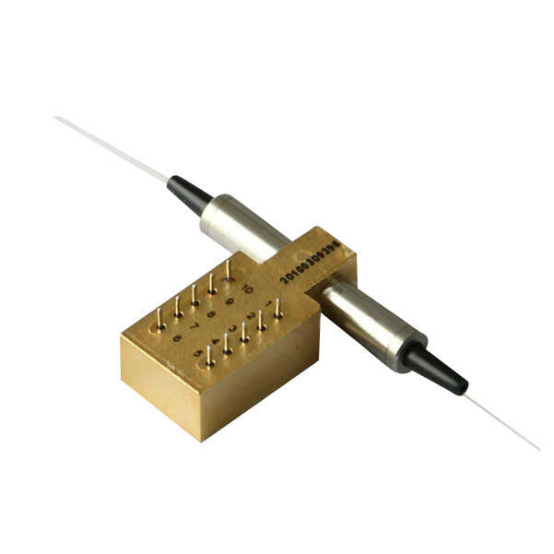
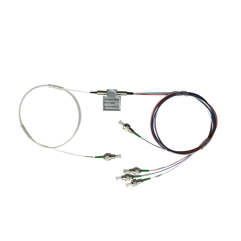
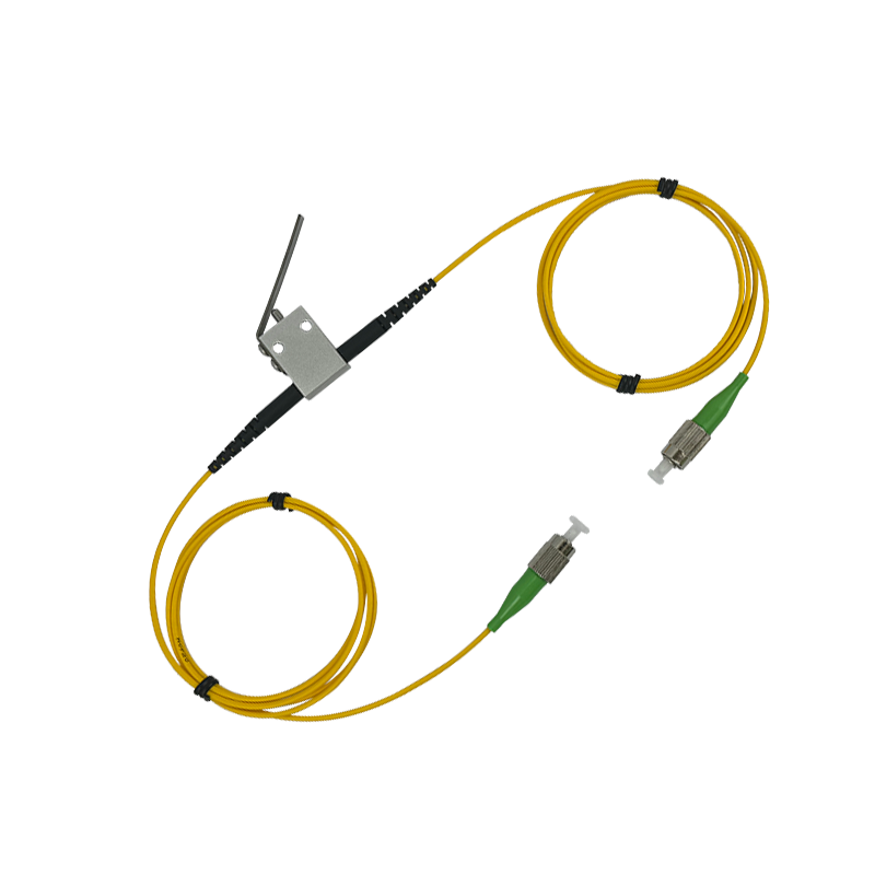
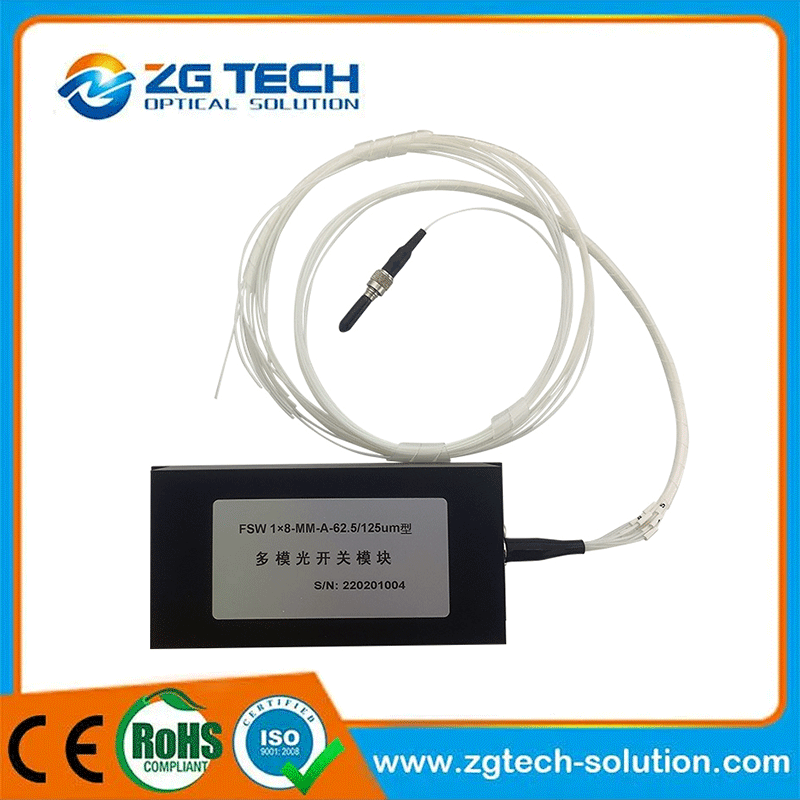
光开关正从传统的机械式向非机械式快速发展。MEMS光开关通过微镜阵列实现光路切换,既保持了机械式低插损(<1dB)的优势,又将切换速度提升至毫秒级。基于液晶技术的波导型光开关进一步将体积缩小到芯片级别,在数据中心光交换中展现巨大潜力。
Optical switches are rapidly developing from traditional mechanical to non-mechanical types. MEMS optical switches use micro-mirror arrays to achieve optical path switching, maintaining the advantage of low insertion loss (<1dB) of mechanical switches while improving switching speed to the millisecond level. Waveguide-based optical switches using liquid crystal technology further reduce the size to the chip level, showing great potential in data center optical switching.
最新研发的热光开关采用硅基光子学技术,将开关单元集成在毫米级芯片上,支持高达128×128的端口配置。这些革命性产品为软件定义光网络(SDON)提供了硬件基础,使网络拓扑可实时重构成为可能。
The newly developed thermo-optic switches use silicon photonics technology to integrate switching units on millimeter-scale chips, supporting port configurations of up to 128×128. These revolutionary products provide the hardware foundation for software-defined optical networks (SDON), making real-time network topology reconfiguration possible.
波分复用技术:突破容量瓶颈的关键
Wavelength Division Multiplexing Technology: The Key to Breaking Capacity Bottlenecks
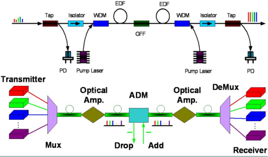
CWDM和DWDM器件继续向更窄信道间隔发展。新一代DWDM模块信道间隔缩小至75GHz,单光纤传输容量突破100Tbps。基于AWG(阵列波导光栅)的复用器采用二氧化硅波导技术,插损降至3dB以下,相邻信道串扰控制在-35dB以内。
CWDM and DWDM devices continue to develop towards narrower channel spacing. The channel spacing of new-generation DWDM modules has been reduced to 75GHz, with single-fiber transmission capacity突破 100Tbps. AWG (Arrayed Waveguide Grating)-based multiplexers use silica waveguide technology, reducing insertion loss to below 3dB and controlling adjacent channel crosstalk to within -35dB.
在城域网应用中,可调谐波分复用器成为新趋势。通过热电冷却器(TEC)和波长锁定技术,这些器件能够实现自动波长对准和温度补偿,显著降低了系统调试和维护成本。
In metropolitan area network applications, tunable wavelength division multiplexers have become a new trend. Through thermoelectric coolers (TEC) and wavelength locking technology, these devices can achieve automatic wavelength alignment and temperature compensation, significantly reducing system调试 and maintenance costs.
测试与创新:保障器件性能的关键环节
Testing and Innovation: Key Links in Ensuring Device Performance
现代光无源器件的测试已发展到智能化、自动化阶段。基于偏振扫描法的全参数测试系统可在30秒内完成插入损耗、回波损耗、偏振相关损耗等多项参数的测量,测试精度达到0.01dB。集成化测试平台通过云边协同架构,可实现远程测试和数据共享,大大提升了研发和生产效率。
Testing of modern optical passive devices has developed to an intelligent and automated stage. Full-parameter test systems based on polarization scanning method can complete measurements of multiple parameters such as insertion loss, return loss, and polarization-dependent loss within 30 seconds, with test accuracy reaching 0.01dB. Integrated test platforms, through cloud-edge collaboration architecture, enable remote testing and data sharing, greatly improving research and development and production efficiency.
人工智能技术正在被引入器件设计和测试领域。通过机器学习算法,系统能够自动优化器件设计参数,预测产品在不同环境下的性能表现,并将测试数据分析时间从小时级缩短到分钟级。
Artificial intelligence technology is being introduced into device design and testing. Through machine learning algorithms, systems can automatically optimize device design parameters, predict product performance in different environments, and reduce test data analysis time from hours to minutes.
应用前景与发展趋势
Application Prospects and Development Trends
随着5G网络的全面部署和数据中心流量的爆炸式增长,光学无源器件正面临新的发展机遇。硅光子技术的成熟使得光子集成电路(PIC)成为现实,将多个无源器件集成在单一芯片上已成为行业趋势。这些高度集成的光学引擎不仅减小了设备体积,还显著提高了系统可靠性和能耗效率。
With the comprehensive deployment of 5G networks and the explosive growth of data center traffic, optical passive devices are facing new development opportunities. The maturity of silicon photonics technology has made photonic integrated circuits (PIC) a reality, and integrating multiple passive devices on a single chip has become an industry trend. These highly integrated optical engines not only reduce equipment size but also significantly improve system reliability and energy efficiency.
在量子通信、传感网络等新兴领域,光学无源器件将继续发挥不可替代的作用。超高精度滤波器、超低损耗交换矩阵等特种器件的发展,将为这些前沿应用提供关键支撑。
In emerging fields such as quantum communication and sensor networks, optical passive devices will continue to play an irreplaceable role. The development of special devices such as ultra-high precision filters and ultra-low loss switching matrices will provide key support for these cutting-edge applications.
了解更多产品信息和技术细节,请访问官方网站 www.optical-solution.com 或联系技术顾问 Yukizgsales1@optical-solution.com
For more product information and technical details, please visit the official website www.optical-solution.com or contact technical consultant Yukizgsales1@optical-solution.com
Does your optical network often experience lag? It may be that the optical switch is "false switching"!
Related Article